hankyoreh
Links to other country sites 다른 나라 사이트 링크
How Samsung’s promises of cutting-edge tech won US semiconductor grants on par with TSMC
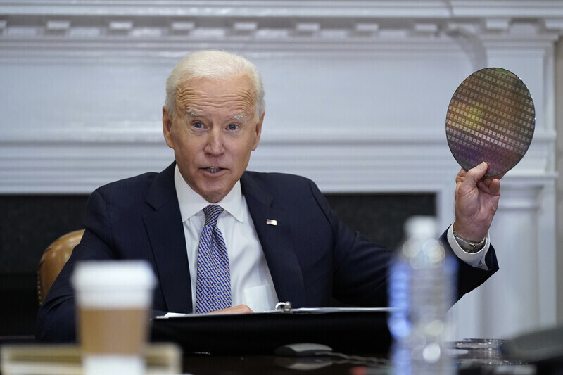
A veritable gift basket offered by Samsung Electronics to the US is seen as one of the factors behind the company’s ability to score large-scale subsidies there.
Samsung Electronics made pledges to establish a state-of-the-art process in the US ahead of the Taiwanese company TSMC and to establish a comprehensive local ecosystem that includes packaging and research and development functions.
In a press release Monday, the US Department of Commerce said the investments would “turn Samsung’s existing presence in Texas into a comprehensive ecosystem for the development and production of leading-edge chips in the United States.”
The reference to a “comprehensive ecosystem” was not included when subsidies for TSMC were announced. At US$40 billion, the investment from Samsung Electronics is smaller than the US$65 billion offered by TSMC — but the use of the phrase suggests a qualitative difference in terms of content.
To begin with, Samsung Electronics plans to establish state-of-the-art processes in the US with little lag time. The company plans to start mass production of 2 nm semiconductors at its South Korean semiconductor fabs next year and to introduce the process in 2016 at its fab in Taylor, Texas. In effect, there will be little time difference between the advanced technology’s introduction at home and in the US.
In contrast, TSMC plans to introduce its 2 nm process to the US in 2028, or around three years after its adoption in Taiwan.
In addition to its state-of-the-art fab, Samsung Electronics also pledged to build various other infrastructure in the US. This was another difference from TSMC, which only announced plans for existing fab expansions.
As a first step, Samsung Electronics plans to build advanced packaging facilities in Taylor — a feature not included in its original plan — and produce the high-bandwidth memory semiconductors used in artificial intelligence.
Packaging, which represents a back-end process for semiconductors, is an area where the US government has expended efforts to build its global market share, which currently stands at around 3%. In particular, it has noted the severe national security and supply chain risks posed when packaging does not take place within its own borders.
Other areas of emphasis included collaboration on security and R&D. The US Department of Commerce said that Samsung Electronics’ proposed investment “also includes commitments to collaborate with the US Department of Defense.”
The company plans to build an R&D fab in Taylor and collaborate with local industries and education institutions.
The Department of Commerce said this would be the first time in history that a foreign company builds an R&D fab in the US.
By Lee Jae-yeon, staff reporter
Please direct questions or comments to [english@hani.co.kr]

Editorial・opinion
![[Column] Season 2 of special prosecutor probe may be coming to Korea soon](https://flexible.img.hani.co.kr/flexible/normal/500/300/imgdb/original/2024/0426/3317141030699447.jpg "[Column] Season 2 of special prosecutor probe may be coming to Korea soon") [Column] Season 2 of special prosecutor probe may be coming to Korea soon
[Column] Season 2 of special prosecutor probe may be coming to Korea soon![[Column] Park Geun-hye déjà vu in Yoon Suk-yeol](https://flexible.img.hani.co.kr/flexible/normal/500/300/imgdb/original/2024/0424/651713945113788.jpg "[Column] Park Geun-hye déjà vu in Yoon Suk-yeol") [Column] Park Geun-hye déjà vu in Yoon Suk-yeol
[Column] Park Geun-hye déjà vu in Yoon Suk-yeol- [Editorial] New weight of N. Korea’s nuclear threats makes dialogue all the more urgent
- [Guest essay] The real reason Korea’s new right wants to dub Rhee a founding father
- [Column] ‘Choson’: Is it time we start referring to N. Korea in its own terms?
- [Editorial] Japan’s rewriting of history with Korea has gone too far
- [Column] The president’s questionable capacity for dialogue
- [Column] Are chaebol firms just pizza pies for families to divvy up as they please?
- [Column] Has Korea, too, crossed the Rubicon on China?
- [Correspondent’s column] In Japan’s alliance with US, echoes of its past alliances with UK
Most viewed articles
- 1‘We must say no’: Seoul defense chief on Korean, USFK involvement in hypothetical Taiwan crisis
- 2Why Kim Jong-un is scrapping the term ‘Day of the Sun’ and toning down fanfare for predecessors
- 3Two factors that’ll decide if Korea’s economy keeps on its upward trend
- 4Gangnam murderer says he killed “because women have always ignored me”
- 5South Korea officially an aged society just 17 years after becoming aging society
- 6BTS says it wants to continue to “speak out against anti-Asian hate”
- 7After election rout, Yoon’s left with 3 choices for dealing with the opposition
- 8No good, very bad game for Korea puts it out of Olympics for first time since 1988
- 9Ethnic Koreans in Japan's Utoro village wait for Seoul's help
- 10US citizens send letter demanding punishment of LKP members who deny Gwangju Massacre